| YEAR |
Milestone |
| 2020 |
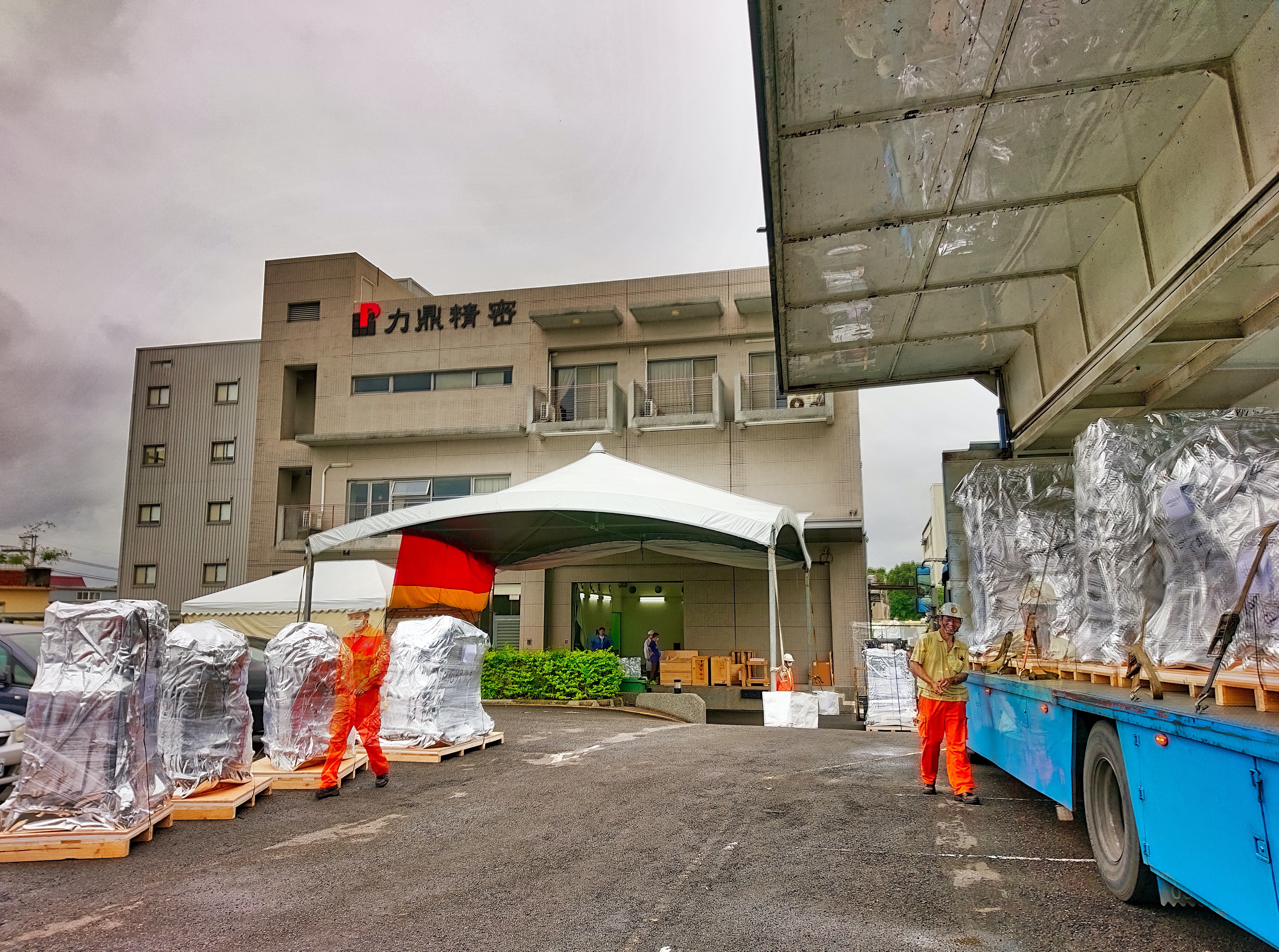
TSMC placed repeated orders for multiple Robusta300+ to fulfill the upcoming production of 5nm wafer Advanced Packaging, new systems for phase one were shipped out on-time.

|
| 2019 |
Robusta300+ became N5 Cu Bump primary PTOR and joined N5 risk-run and Tape-out qualification.
Super Mini Batch Degas (MBD 2) chamber won the 26th Taiwan SMEs Innovation Award.
|
| 2018 |
Robusta300+ joined major production of UBM/RDL in Advanced Packaging Fab 2 (AP02) TSMC.
Robusta300+ passed MTBC 8,000 production record and significantly extended PM cycle time.
Robusta300+ also processed ultra low contact resistivity application for major customers at AP02.
LPI has been assessed and certified as meeting the requirements of ISO9001:2015.
|
| 2017 |
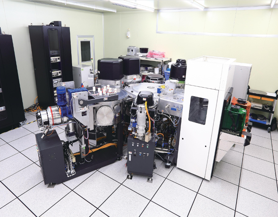
LPI08190 shipped to Semiconductor Manufacturing International Corporation China for TSV process development and production.
TSMC bought the 5th Robusta, LPI12188, for new process production in Bump Line Fab. in Tainan.
Robusta®300 became a primary production tool of 7nm generation IC packaging.
ChipMOS bought GriFfin chambers for Si-Trench TiW / Au production.
Union Semiconductor Co. Ltd. China bought the 3rd Robusta for Wafer Level Gold Bump Packaging production.
|
| 2016 |
LPI12168 passed process and particle qualification on high outgas substrates of Polyimide, Molding Compound, PR, and Glass/Si Composited wafer.
Both LPI12182 and LPI12168 joined formal production in TSMC.
LPI12168 passed qualification and became the primary PTOR for 7nm generation IC packaging.
ChipMOS bought the 16th Robusta for Gold Bump and Solder bump production.
|
| 2015 |
LPI introduced ISO 9001:2008 Quality management systems.
LPI12183 shipped to Long-Tan Fab. TSMC for production of InFO qualification.

|
| 2014 |
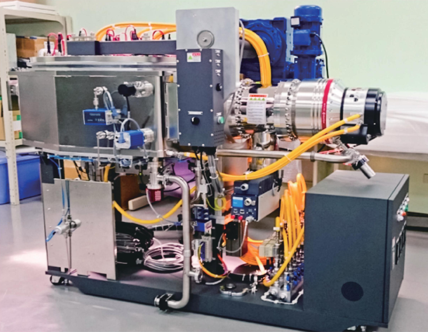
LPI12168 joined Integrated-Fan-Out process development and production qualification at TSMC.
TSMC bought the 3rd Robusta for Bump Line Fab. in Tainan.
ChipMOS bought the 14th Robusta for Gold Bump and Solder bump production.
|
| 2013 |
LPI12168 developed and tested metallization process specifications for high outgas substrate with TSMC supports at Fab 7.
LPI12168 passed Bumping metalization process on Polyimide and production qualification at F7 Bump Line, TSMC.
|
| 2012 |
Caprica started to perform Caparica Deep Silicon Etch and Oxide Etch process development and production qualification in Advanced Semiconductor Engineering Group.
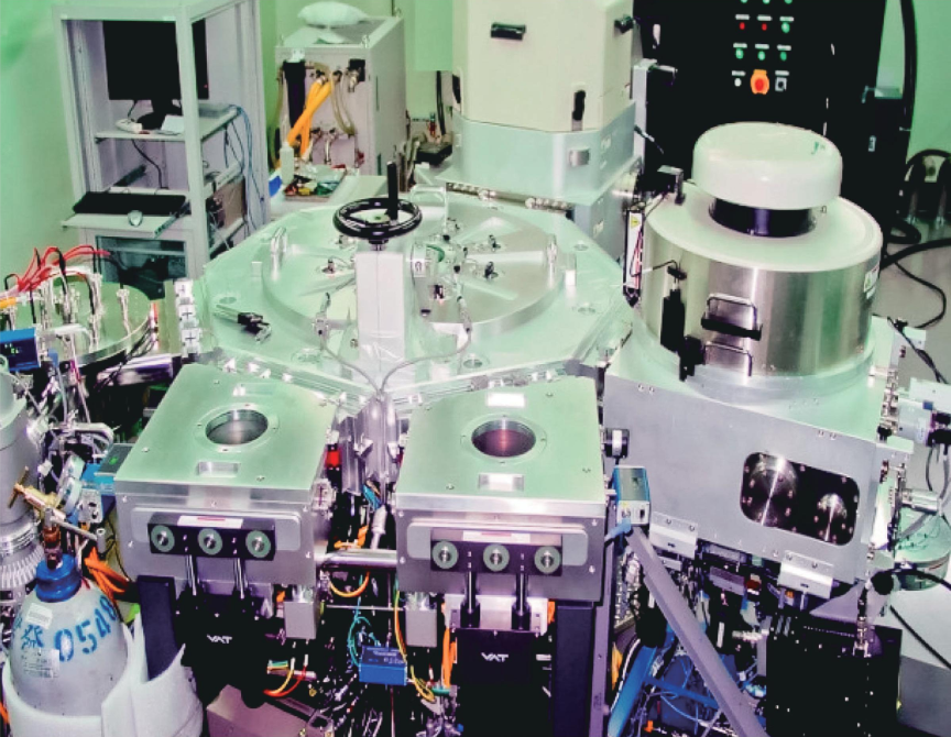
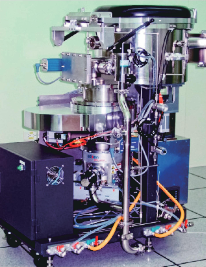
Robusta®200 shipped to Union Semiconductor Co. Ltd. China for Wafer Level Gold Bump Packaging production.
LPI12168 kicked off process development for Wafer Level Bumping on Polyimide (PI) substrate, a major material in current Bumping industry.
Customized LPI12176 shipped to Semicat, Inc. in Korea for process development of advanced memory devices.
Customized LPI08181 shipped to MPI Corporation, Chu-Pei City, Taiwan, and developed non-wafer type substrates sputtering capability.
ChipMOS bought the 10th Robusta for Gold Bump and Solder bump production.
TSMC Solid State Lighting bought 2nd Robusta for LED production.
|
| 2010 |
Customized Robusta®200 shipped to TSMC Solid State Lighting for LED production.
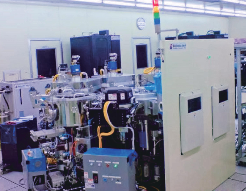
LPI12171 shipped to ADL Engineering Inc. for production, first tool with in-situ interchangable capability between 200mm and 300mm.
ChipMOS bought its first 300mm wafer level production tool for 300mm wafer Gold Bump production
Caprica 300 Deep Silicon Etch released.
|
| 2009 |
Caprica 300 Deep Silicon Etch system received Funding from Industrial Development Bureau, Ministry of Economic Affairs for Development of Leading Product Project.
Lewis330 Sapphire Etcher shipped to Touch Micro-System Tech. for Microelectromechanical Systems production development.
Robusta®300 GriFfin System received Funding from Ministry of Science and Technology.


|
| 2008 |
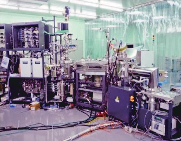
Robusta®300, LPI12168, moved in TSMC for Demostration of production.
Customized 300mm system, shipped to TSMC and worked with Explore R&D for 20nm Automic Layer Deposition Hi-K and metal gate, Co-Sputter, and Post Dep. Anneal process development.
LPI introduced the ERP system for increasing operation efficiency.
LPI kicked off the development of Caprica 200 Deep Silicon Etch system.
|
| 2007 |
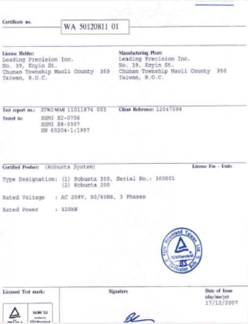
Leading Precision Inc. released Robusta®300 and passed SEMI S2 compliance.
Leading Precision Inc. was established.
Leading Precision Inc. (LPI) built headquarter facility in Jhu-Nan Township, Miao-Li County, Taiwan.
LPI’s project of 300mm Physical Vapor Deposition for Under Bump Metal received Funding from Industrial Development Bureau, Ministry of Economic Affairs for Development of Leading Product Project.

|
| 2006 |
Robusta®200 formally joined Gold Bump production, high-end Chip Scale Wafer Level Packaging, in ChipMOS TECHNOLOGIES INC. Taiwan.
CSS shipped two systems to ChipMOS TECHNOLOGIES (Shanghai) LTD. in China for high-end Chip Scale Wafer Level Packaging.
|
| 2005 |
CSS kicked off the development of IC Wafer Level Packaging production equipment and system.
|
| |
|